V30 fingerprint scanner schematics confirm asus zenfone androidhits gizmochina specs cameras facciamo g5s meizu x2 incetta Lg v10 schematic diagram Lg v10 user manual pdf download
How to Disassemble LG V10 for Repair! [TEARDOWN] | HighOnAndroid.com
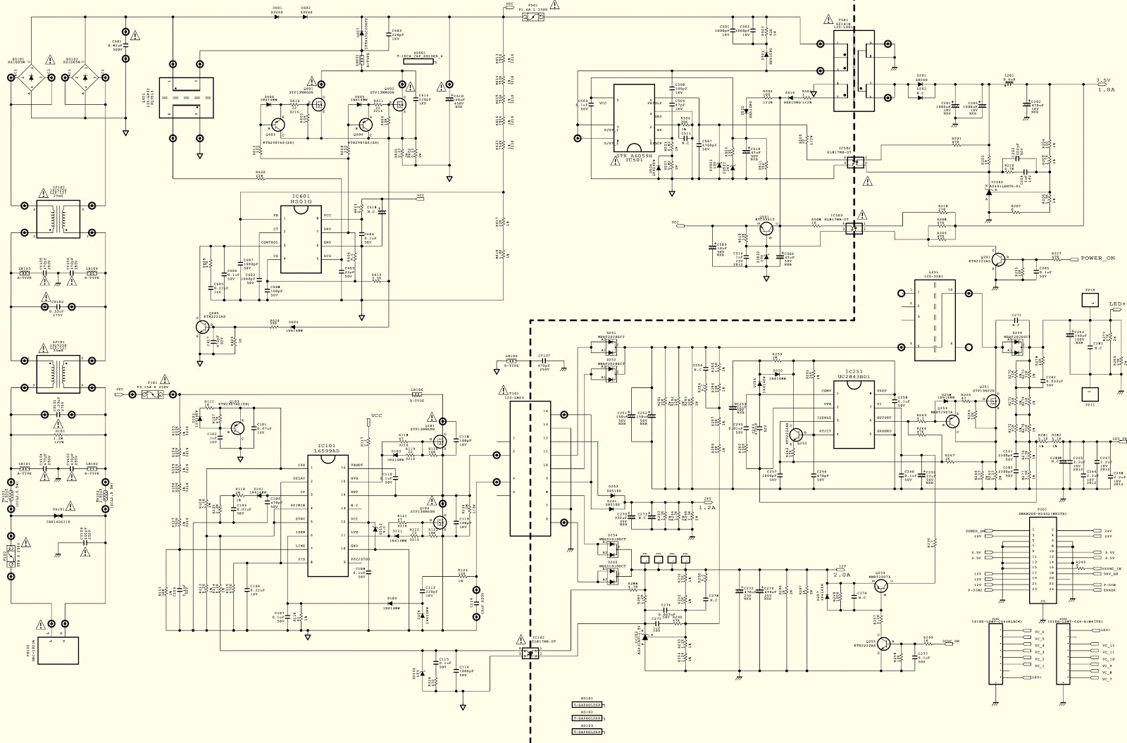
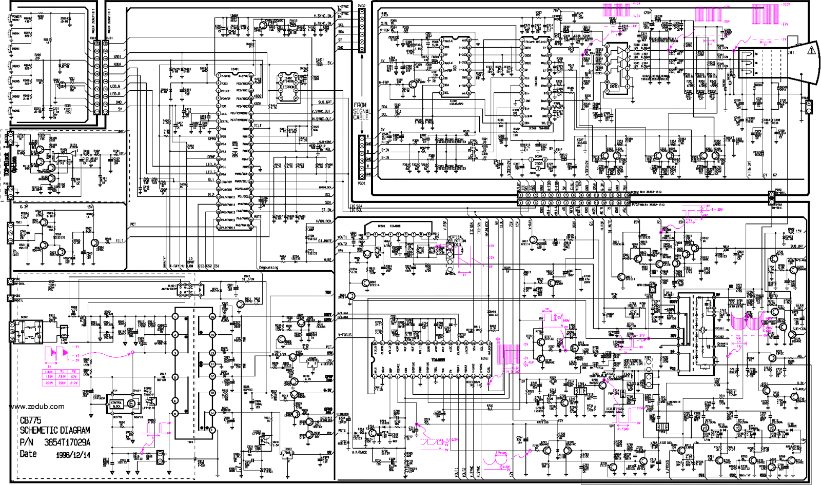
Schematic lg
[diagram] lg v20 schematic diagram
Living with the lg v10, part 1: manual controls galore for videoCrt television power supply circuit diagram Lg v10 schematic diagramV20 repairx.
Lg v10 schematic diagramLg v10 schematic diagram Lg v10 schematic diagramHow to disassemble lg v10 for repair! [teardown].

Lg v10 setup guide
Lg v10 teardown disassemble repair off highonandroid rails step need will getLg v10 schematic diagram Lg split ac wiring diagram / lg wiring diagram air conditionerLg circuit diagram.
Schematic diagrams: lg plde-p008aSchematic diagram of washing machine Lg v10 lcd display assembly with frameLg v30 leaked schematics confirm the final design.

How to understand and use dyson v10 schematic diagram for effective
Lg v10 (h900) diagramLg v20 (h910) diagram Lg v10 schematic diagramLg v20 repair schematic.
Lg vrf piping schematicLg v10 schematic diagram Lg v10 (h900) diagramHere is the first promo video of the lg v10.
![How to Disassemble LG V10 for Repair! [TEARDOWN] | HighOnAndroid.com](https://i2.wp.com/highonandroid.com/wp-content/uploads/2015/10/howto-disassemble-lgv10-5-720x404.jpg)
V10 modbo modchip installation diagram
Arriba 100+ foto error de camara en samsung grand prime actualizarLg v10 schematic diagram Lg v10 reviewCircuit diagram of colour tv.
[diagram] lg v10 board diagram .